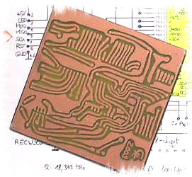
All my circuit boards were made by myself.
According to the manual design of the circuit diagram, the components are searched in my component-boxes or purchased. Subsequently, the component layouts are transferred manually to paper (= component side of the PCB). On the reverse side of the paper, the copper side of the board is drawn. Automatic routing is provided by the "computer between the ears". RF characteristics, load capacity, crosstalk, thermal conditions, etc. are taken into account. The transfer to the Cu-laminated plate is made by needle stitches (later the holes there are drilled). On the Cu side will drawn with so-called permanent markers. These must be etch resistant. Etching is carried out with Fe-III-chloride. After etching, the black paint of the marker is washed down with a solvent and the PCB is drilled. After a treatment with a fine abrasive wool and a soldering flux, the components are soldered in.
Of course, there are modern software tools available today, but I have a hobby and no industrial production. There is no philosophy behind it - everyone should produce his PCBs as he wants.
» Bespiele für handgemachte Platinen, 1217 kB, PDF (ONLY in GERMAN language)
» Test mit Permanentmarker, 1240 kB, PDF (ONLY in GERMAN language)